In the field of semiconductor manufacturing equipment, since 2015, when the era of big data entered, the US market size of dry etching equipment has surpassed that of lithography equipment, becoming the largest, exceeding $12 billion annually in 2021.
A dry etching apparatus includes a consumable member called an edge ring (focus ring).
In the old days, the material of the edge ring was quartz. However, at present, quartz is no longer used due to its lack of durability, ceramics with even higher hardness such as SiC are often used.
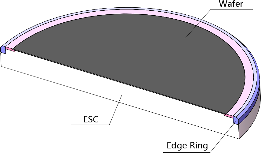
Role of the edge ring
- It is to protect the lower structure of the edge of the ESC of the stage on which the wafer is placed from the plasma.
- By placing an edge ring of insulator around the periphery of the wafer, the non-uniformity of the etching characteristics around the periphery of the wafer is reduced.
AST's consumable parts processing business for dry etching equipment is centered on ceramics and silicon parts processing.
Ceramic processing
We provide various ceramic parts using our material, production, and precision processing technology for high-strength, high-purity ceramics. The main products are ceramic edge rings/plates for dry etching equipment.
Ceramic products is divided into fine ceramic products (FC), which have excellent properties such as high strength, high purity, and high heat resistance, and machinable ceramics (MC), which is machined in an advanced manner. The former is mainly used for semiconductor manufacturing equipment and is an indispensable part of the dry etching method (plasma etcher). The latter is used as various parts and jigs after being processed in multiple ways and is especially in demand as jigs (for wafer probers) in the semiconductor inspection process. In recent years, it is also being used in advanced medical equipment by taking advantage of its precision processing characteristics.
Our company's characteristics
Silicon parts processing
We manufacture embedded parts for semiconductor manufacturing equipment, mainly monocrystalline and polycrystalline silicon products. Our primary focus is silicon for contact electrodes used in dry etching equipment, silicon edge rings/plates, etc.
Silicon parts (ports, injectors, focus rings) are processed and used mainly in the semiconductor manufacturing process. In addition to being used in wafer film formation and diffusion processes, they are also used as jigs and consumables in the transportation and cleaning processes. They play an essential role in the semiconductor manufacturing process where miniaturization and high purity are progressing.
Our company's characteristics
Many of the machining processes in the factory are vertical Maching Centers (MCs), and there is a need to accelerate automation due to many complications.
The processing process includes the arrival of ceramic and silicon materials, surface grinding, inner diameter and outer shape processing using a machining center (MC), plate drilling, followed by cleaning and shipping. Many parts are imported from Asia. In MC processing, which is the main focus, there are many small vertical MCs, and specifically, many of the machines manufactured by JTEKT and OKK are in operation.
AST is advancing automation and unmanned MC processing. We currently have several automated lines in operation. We are also working to save space and extend automated processing times to improve factory productivity.
A research company predicts that the dry etching equipment market will expand by an average of 8% in the future, but some equipment manufacturers are forecasting an even stronger demand. Multilayering is further progressing in 3D NAND flash investment and the current cutting-edge 3. DNAND has 112 to 128 layers, and the number of layers is expected to increase 1.3 to 1.5 times each year. As demand rises and the etching time per wafer grows, increasing the number of dry etching equipment or chambers per equipment is the only solution.